Microelectronics industry
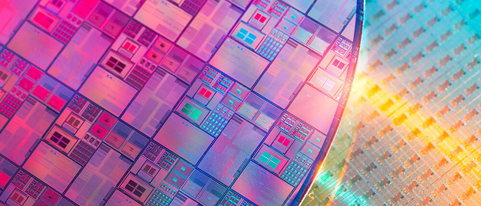
Profilplast offer a comprehensive portfolio for the handling and automation of high purity applications. Our staff has more than 30 years of experience in microelectronic process & product solutions.
Applications
- Wet etch and clean
- Chemical mechanical planarization (CMP)
- Physical vapor deposition (PVD)
- Chemical vapor deposition (CVD)
- Substrate doping
- Photolithography
- Epitaxy
- Particle characterization
- Temperature control
- Substrate handling
More information?
For more information and technical support, please contact our product specialists. We are happy to help you!
+49 (0) 7704 923 7940